Grain engineering for improved charge carrier transport in two-dimensional lead-free perovskite field-effect transistors
Controlling crystal growth and reducing the number of grain boundaries are crucial to maximize the charge carrier transport in organic–inorganic perovskite field-effect transistors (FETs). Herein, the crystallization and growth kinetics of 2D perovskite, were effectively regulated by the hot-casting method. Our work provides an important insight into the grain engineering of 2D perovskites for high-performance FETs.
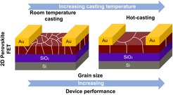
One of the main obstacles in achieving a reliable operation of perovskite transistors at room temperature is severe ion migration, which can screen the applied gate field, resulting in poor field-effect behavior and large dual-sweeping hysteresis. Grain engineering controlled by film deposition parameters is one of a new approach to improve charge carrier transport and understand the relation between crystallization and ions migration. Such processing condition like substrate temperature are usually not consider as a powerful tool to control surface morphology and microstructure. In this work, hot-casting method is used for an effective modulation of grain size and grain boundaries number, in order to improve in-plane charge carrier transport in perovskite film. Additionally, a close correlation between the density of grain boundaries, charge carrier transport, and ion migration is established. We believe that the grain engineering proposed herein is a major breakthrough for developing operationally stable room-temperature perovskite transistors.