Defects to the rescue: Exploiting defects at Van der Waals interfaces between layered materials
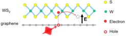
 before being trapped and stored at vdW interfaces. This results in a long-lived (> 1 ns) photogating effect in graphene.")
Following photoexcitation and interfacial charge transfer, the injected electrons only occupy the excited states of WS2 shortly (~1 ps) before being trapped and stored at vdW interfaces. This results in a long-lived (> 1 ns) photogating effect in graphene.
Van der Waals (vdW) materials, such as graphite and transition metal dichalcogenides (TMDs, e.g. WS2), are layered materials made up of strong two-dimensional (2D) sheets that are weakly bound in the third dimension through vdW forces. Owing to the weak interlayer interaction, atomically thin vdW monolayers can be produced via mechanical exfoliation. The most notable example is graphene, a monolayer of graphite, produced by peeling off layers from the bulk using simple scotch tape. Graphene is a semimetal, and exhibits extremely high charge carrier mobility, making it relevant for electrical devices. Other vdW monolayers, e.g. those exfoliated from TMDs, are usually semiconductors which are also useful for many optical and optoelectronic applications. 2D monolayers from different materials can be stacked vertically to form so-called “vdW heterostructure”. Heterostructures consisting of graphene and TMDs have recently shown great promise for high-performance optoelectronic applications. For instance, the integration of graphene and monolayer WS2 enables sensitive photodetectors with ultrahigh photoresponsivity, by combining strong light absorption in WS2, efficient charge transfer across the interfaces, and superior charge transport properties in graphene. Currently, devices are mostly developed through trial-and-error since an in-depth understanding of interfacial charge transfer and recombination has so far remained elusive, limiting the optimization of device performance.
, the interfacial defects (e.g. sulfur vacancies) can “capture” (the red solid line) and “store” the injected electrons, leading to an extremely long-lived charge separation and thus an interfacial electrical field (E) to effectively gate graphene.")
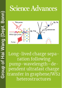
Researchers from the Max Planck Institute for Polymer Research, in collaboration with partners from Delft University of Technology, the University of Electronic Science and Technology of China, Zhejiang University, and the Catalan Institute of Nanoscience and Nanotechnology, now shed light on these processes in graphene-WS2 heterostructures. The researchers follow the dynamics of charge carriers in the heterostructure by monitoring charges in both graphene (by terahertz spectroscopy) and WS2 (by transient absorption dynamics) on sub-picosecond (ps, =10-12 s) time scales. Combining these two ultrafast techniques, they demonstrate that defects, usually detrimental for device applications, can be beneficial for practical applications of graphene-WS2 vdW structures. These defects at interfaces can be exploited to “capture” and “store” charge carriers, which are transferred across the heterojunction. The study unveils new injection and recombination pathways in graphene-TMDC heterostructures and demonstrates the beneficial effect of interfacial defect states for promoting an extended interfacial charge separation time in graphene-based vdW structures. Understanding such injection and recombination pathways is important for both fundamental studies and optoelectronic applications. For instance, the long-lived charge separation reported here makes graphene-TMDC heterostructures promising for efficient photodetectors. In addition, based on the results, we expect that further defect engineering can provide a versatile and powerful strategy to optimize device efficiency. The results are published in the journal “Science Advances”.


